PCB Manufacturing · 02
PCB manufacturing
Density aligned with leadsintecgroup.com/pcb-manufacturing: board types, materials, process framework, DFM. No carry-over of “up to 32/40/46 layers” or shop-floor areas until unified.
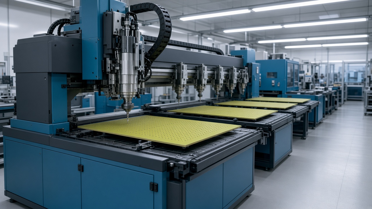
Board types (menu)
- Single / Double side
- Multilayer PCB, including HDI
- HDI as a capability direction
- Impedance-controlled — after engineering confirmation
- Metal-base / aluminum — per project
- High-frequency / RF materials: Rogers, Isola, Taconic, Panasonic… (examples)
Surface finishes
ENIG, OSP, immersion silver / tin and others — a menu, not a promise of every option on every lot.
Process (framework)
As on the group “Advanced PCB Manufacturing Process” — steps without invented hours.
1. Engineering / DFM
Gerber and stack-up review
2. Materials
Incoming materials check
3. Inner layers
Inner layers
4. Lamination / drill
Lamination and drilling
5. Plating / imaging
Copper and imaging
6. Surface finish
Surface finish
7. Optional SMT
Handoff to PCBA line
8. Test / pack
Electrical test and packing
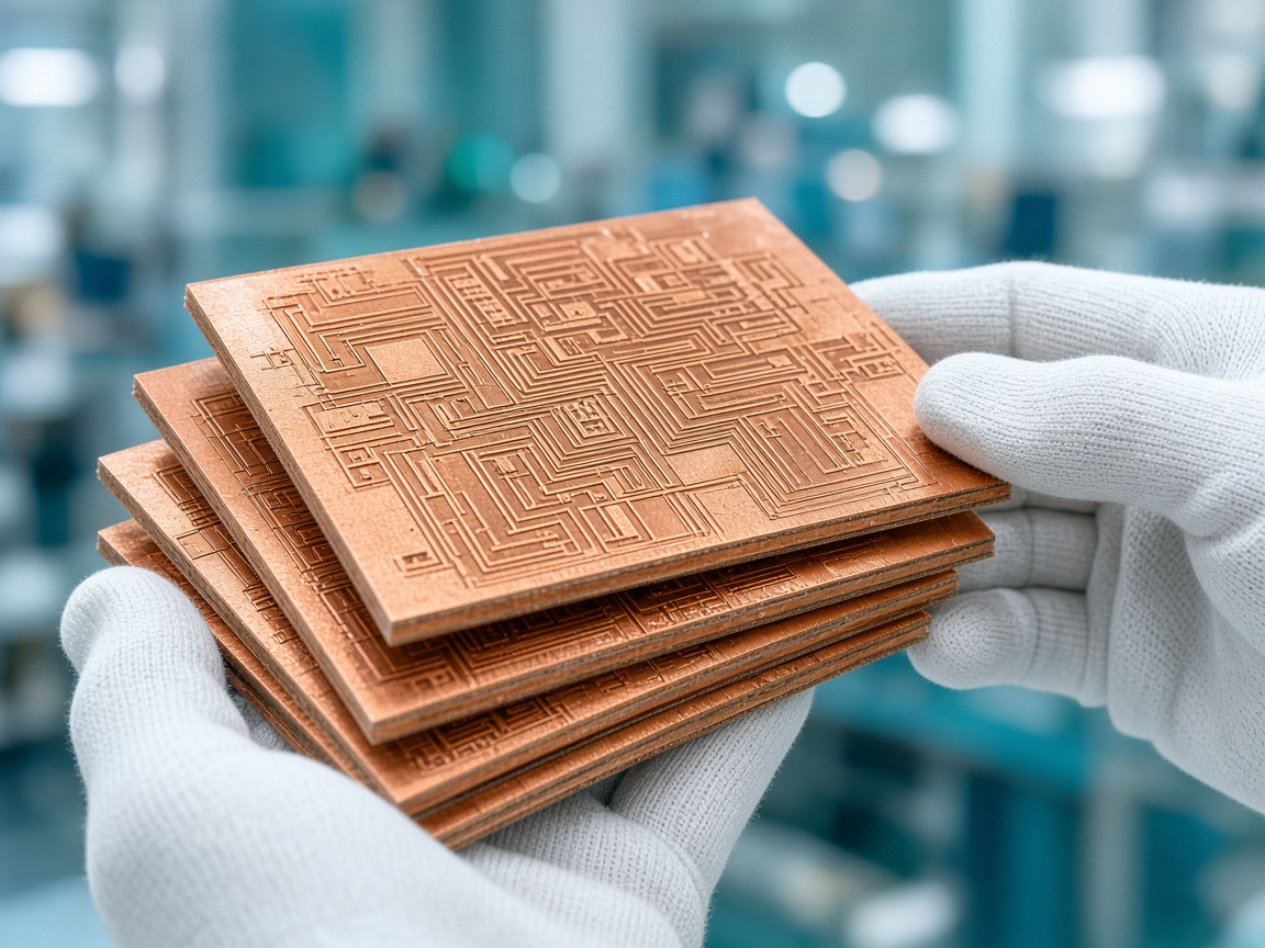
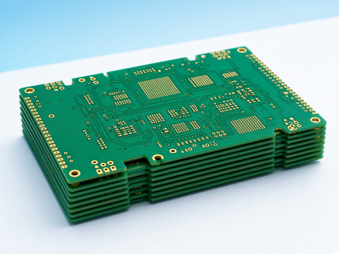
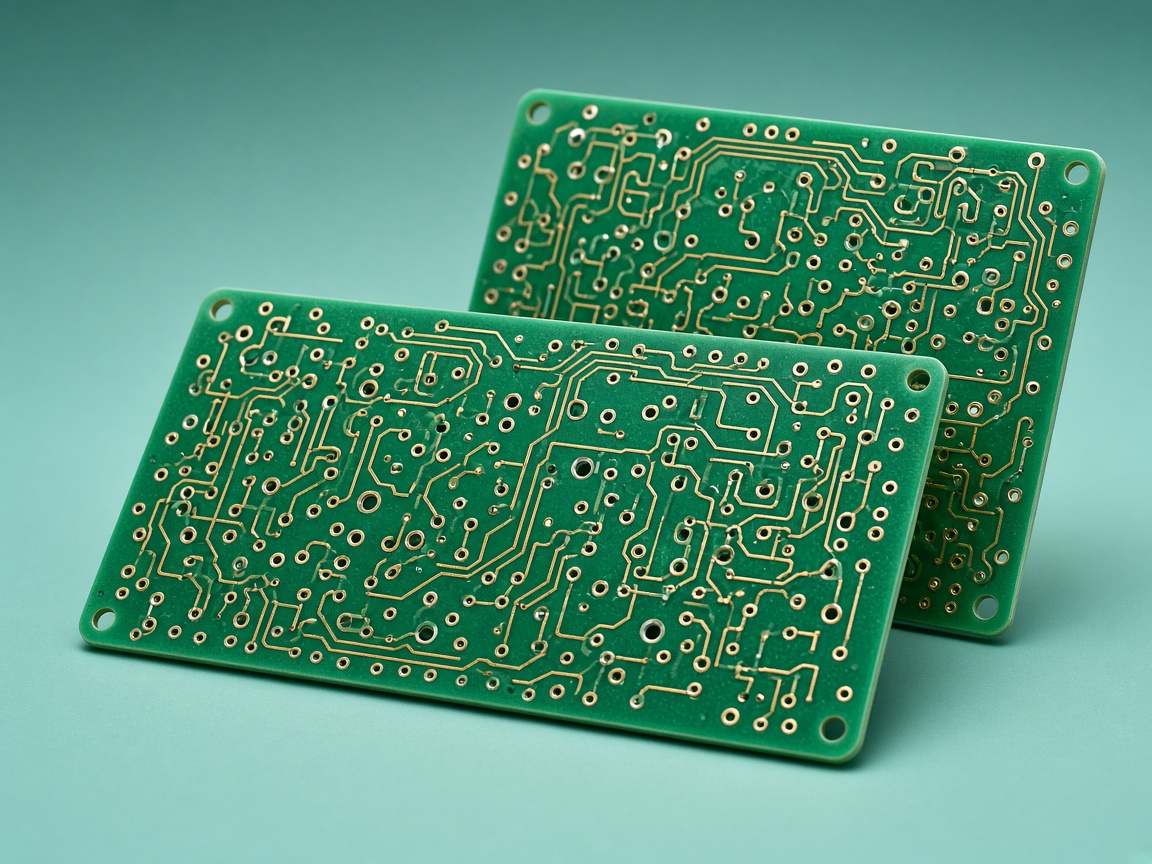
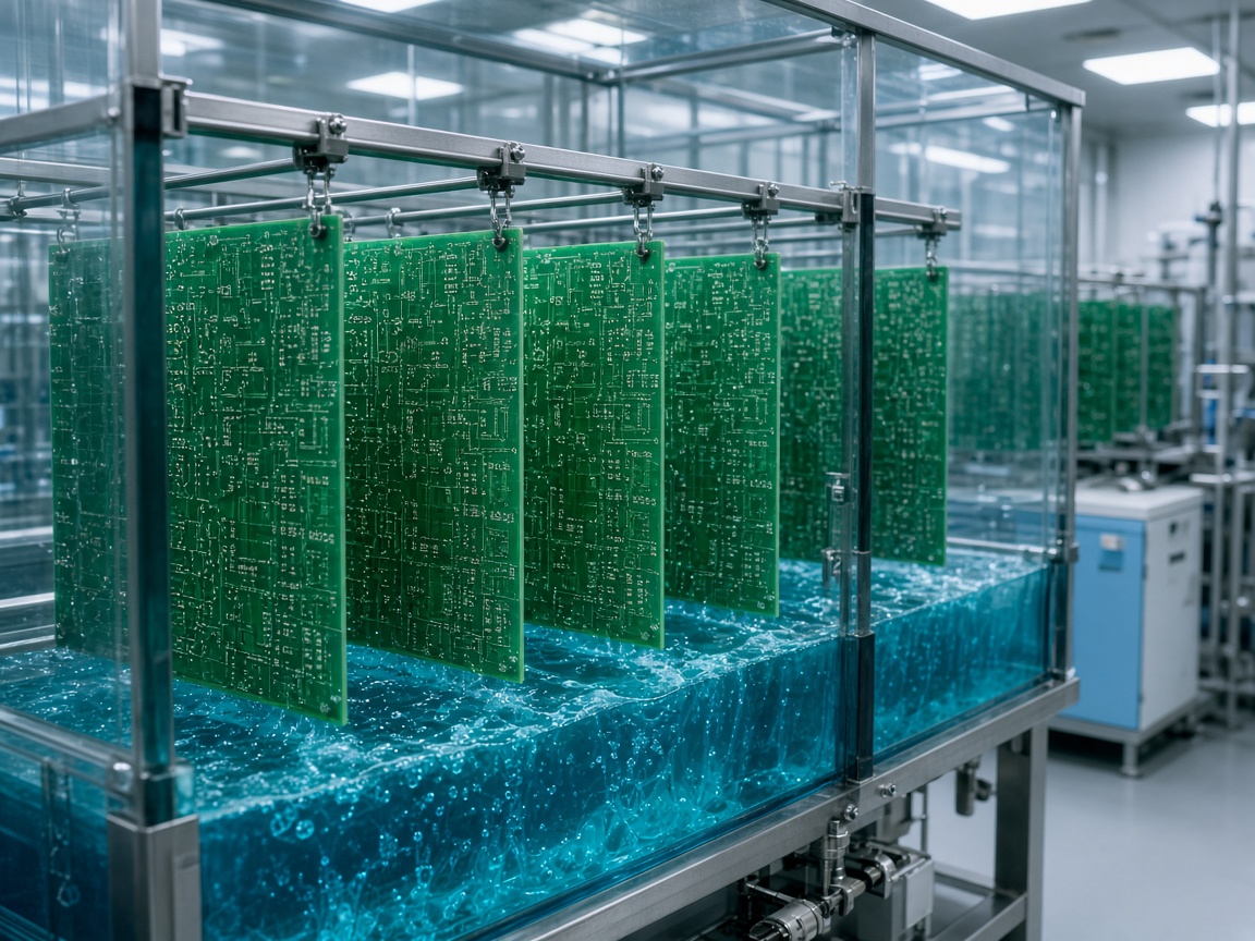
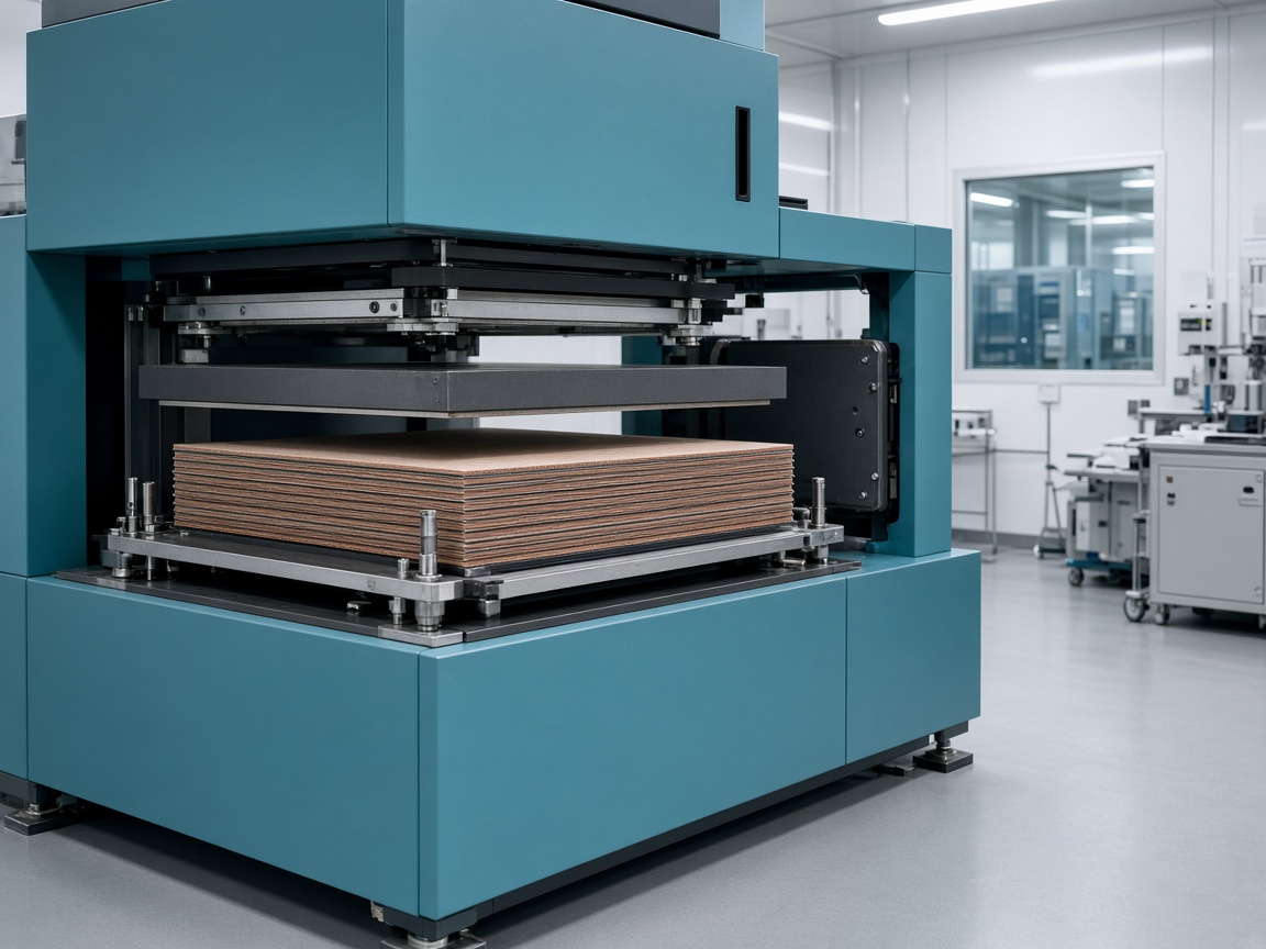
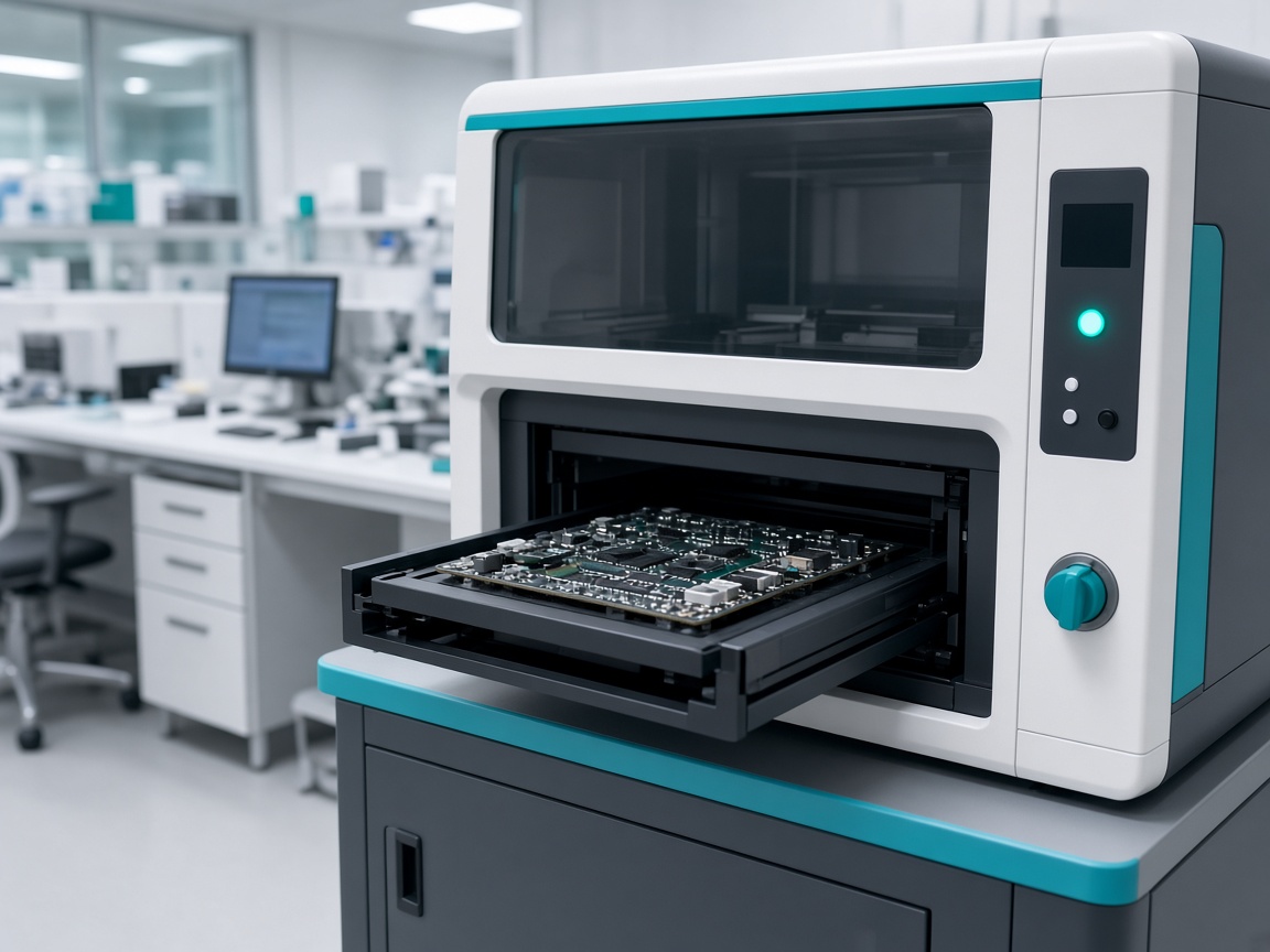
DFM before launch
We check layer completeness, width/spacing risks and stack-up. We do not publish a fixed ‘free within N hours’ SLA.
Quote for board fabrication
Attach Gerber and briefly describe stack-up/finish.